On 2 May 2020, the IPVF* and the CEA launched a joint programme in the photovoltaic field at the INES (Institut National de l’Énergie Solaire - National Solar Energy Institute). The objective of this collaboration, "Tandem Made in France", is to accelerate the development of cells combining perovskite materials with silicon heterojunction technology in order to create a high efficiency tandem device, which can be translated to an industrial scale.
Context: the Tandem principle
In the PV field, very significant technological and economic progress has been seen in recent years, particularly in silicon technology. However, the cells have a theoretical efficiency limit of 29%, reaching up to 26.7% in the laboratory, with little room for improvement.
Achieving very high performance at a controlled cost will therefore inevitably require technological breakthroughs.
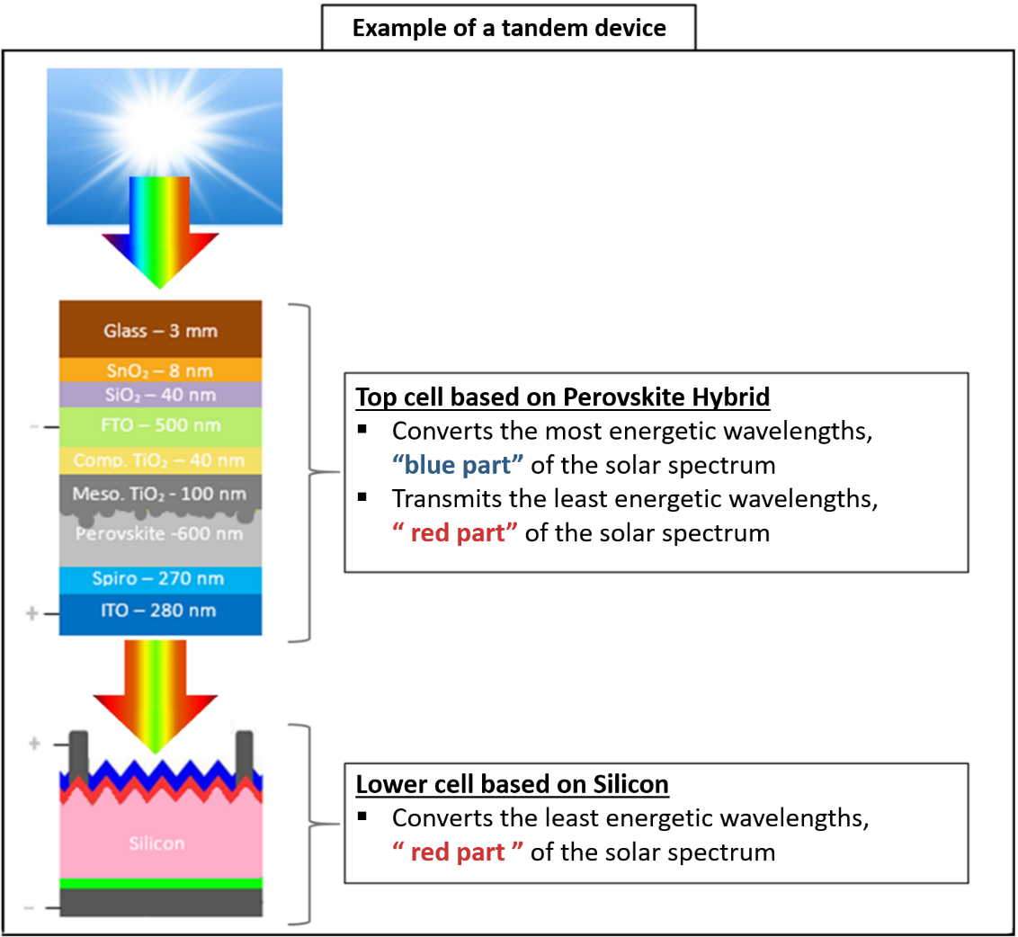
One of the most promising consists of vertically combining two different PV technologies in order to optimise the conversion of the solar spectrum. This principle is known as Tandem, and would allow the theoretical achievable efficiency to be pushed to 42%.
The technology is evolving: hybrid perovskites
Among the various candidates that can be associated with silicon technology, hybrid perovskites are particularly interesting. This technology has developed strongly over the last 10 years and a considerable research effort has made it possible to rapidly achieve high efficiencies (and to catch up with the level of the most advanced technologies).
For example, a record of 25.2% was obtained for small surface area cells (< 1 cm2) by a collaboration between Korean (KRICT - Korea Research Institute of Chemical Technology -) and American (MIT - Massachusetts Institute of Technology -) groups. One of the strong points of hybrid perovskites is the possibility of depositing them in thin layers using atmospheric processes at low temperature, which suggests very low production costs. In addition, the great versatility of these materials allows their optoelectronic properties to be finely tuned to the targeted application; in our case the construction of tandem devices in combination with Silicon.

The R&D work and research partnerships
Working through the IPVF, EDF was able to quickly identify this topic with initial work carried out at the end of 2013, which allowed the creation of a dedicated project in early 2015. Since the beginning of this year a new research programme has been initiated specifically on the use of perovskite hybrids in a tandem device. In particular, this is directed towards solving the problems that currently limit the deployment of this technology on a large scale: a stability that is still too low and the difficulty of making homogeneous deposits on large surfaces, which leads to a drastic drop in efficiency when the size of the devices increases. This research effort has enabled us to acquire a high level of expertise in the deposition of layers, the manufacture of devices and their characterisation.
In parallel, the CEA at INES has developed a silicon-based solar cell technology (called a heterojunction cell) that has very high performance and is particularly well suited to its incorporation as the bottom cell of a tandem device. The INES has also undertaken R&D work on perovskite technology and obtained very interesting results.
The aim of this collaboration is to promote exchanges between the IPVF and the INES in order to combine the complementary skills of these two institutions and to be able to develop breakthrough innovations in order to reach and exceed 30% efficiency while controlling the manufacturing costs of such cells. The aim is also to position ourselves among increased global competition and ultimately to enable the emergence of a competitive French technology.
Contact : Jean Rousset, research engineer on EDF R&D solar technologies
*IPVF : Institut photovoltaïque d’Ile de France (Ile de France Photovoltaic Institute)

